This Saturday, I woke up to the following on the Dragon Sector IRC channel:
Introduction
Let’s take a look at the task description:
ButcherCorp has developed an extremely reliable radiation-hardened IC packaging process. Its only drawback is requiring the ASIC to be fabricated using a specific 0.35μm technology, considered outdated by today’s standards. The intel we gathered suggests that their standard cell library is based on osu035.One of our operatives managed to exfiltrate a GDSII file ButcherCorp has sent to a silicon fab. Apparently, it is the IC responsible for validating the launching code in their latest rocket engine.The IC samples the in
pinat theclock‘s positive edge. If the correct sequence of bits is presented to the IC, it drives theunlockedpin to a high logical level. Find this sequence. It forms an ASCII string which you should submit as a flag.
So, we are given artwork of lithography masks for a VLSI ASIC (a.k.a. integrated circuit) fabricated in AMI 0.35µm technology using the Oklahoma State University OSU035 open source flow. The chip is a simple three-terminal device: a clock and in pin to receive a bitstream of a flag, and an unlocked pin that goes high if the bitstream is correct. We have to reverse engineer it to find the key.
The file is in GDSII/GDS2 format – an industry standard file format for exchange of lithography masks of integrated circuits, mostly used as en exchange format between EDA suites and as an output format given to silicon fabs by hardware designers.
The challenge ASIC is fabricated in Standard Cell technology – this means, in very simplified terms, that the software that converts a digital logic definition file (in RTL form) has a bunch of different ‘cells’ to choose from (ie. AND, NOT, D-Flip-flop, etc…), which it places in a grid and then connects with metal layers to form the final integrated circuit. The library of standard cells used in this task is OSU035.
A quick refresher on the physical topology of a VLSI circuit:
 |
| By Cepheiden, CC BY 2.5, via Wikimedia Commons |
What we’ll bee mostly looking at today is the ‘BEOL’ (back-end of line) section of the chip – the metal interconnect section that wires together the silicon (in the FEOL) of the standard cells together. These metal interconnects consist of a number of planes/layers with vias that connect them together and tungsten pins that connect them to the silicon of the lower layers.
 |
| By David Caron, CC BY 3.0, via Wikipedia |
Let’s load the mask in KLayout, an open source GDSII viewer:

Well, that’s a bit of a soup. Let’s copy over layer name/number mappings from osu_stdcells/lib/ami035/abstract/ami035_layers.map and reorganize them a bit. And zoom in a bit.
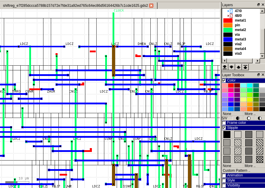
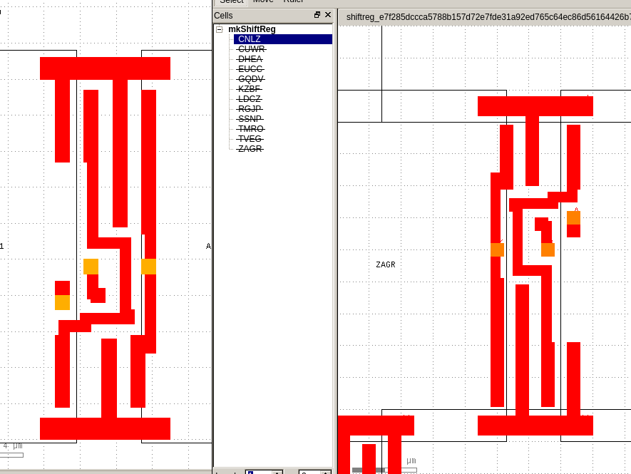
We can see the instantiated cells (for example, three ‘LDCZ’ cells on the top left) represented as boxes with their contents hidden (they are metal 1, pins and silicon layers), and global metal 1-4 layers and vias that join those layers together (visible). If we change display settings, we can peek into some of those standard cells and see how they’re implemented.
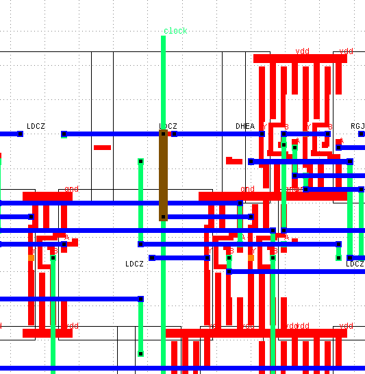
Here we can see instances of the ‘CNLZ’ standard cell metal 1 layer (in red), instantiated multiple times into the design. Some of the instances which are flipped vertically (to fit them across power rails in the design) or horizontally (to better route metal signals).
But what is the logical function of this CNLZ cell? We could go about reverse engineering it at gate-level (by inspecting its’ silicon layers). However, if we open osu035_stdcells.gds2 from the OSU035 files, we can see that it’s in reality AND2X2 (a 2-to-1 AND gate), just renamed and oriented differently during instantiation.
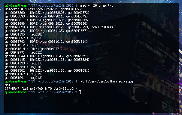
We can now spend around half an hour and map the obfuscated cell names from the challenge GDSII into OSU035 cell names and their logical functions from the cell definition file. I also took the time to note down coordinate of the pins (i.e. A, B, Y, D, Q, CLK …) and their names, so that we can map the I/O of the cells later on.

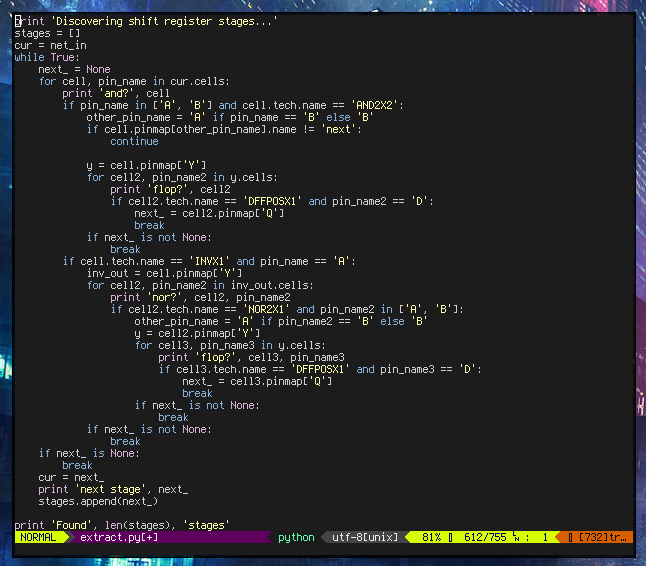
Now, here comes the hard part. We know what cells are used, and where. But we also want to know how they’re connected, so we can reverse engineer the logic of the chip.
What we need is a netlist – a description of all the electrical nets in the design and how they connect all the logic cells together. There’s a few ways to go about this:
- Use a commercial EDA suite (like Cadence or Synopsys) to perform netlist extraction.
- Learn to use Magic VLSI.
- Build your own fucking birdfeeder.
How To Perform Netlist Extraction In Three Easy Steps
Step 1 – combine GDSII rectangles (boundaries) in all metal layers into ‘segments’
Our first job is to turn these into collections of rectangles on metal layers into objects that represent an electrically connected trace, which I called ‘segment’.
Here’s how I did it:
- I loaded the GDSII file, transformed every metal rectangle into a slightly larger bounding box (because I wanted to use bounding box collision detection to connect metal boundaries that might be just slightly touching).
- For every cell/structure of the design, I instantiated the structure’s metal rectangles as well, after transforming them accordingly to flips/rotations.
- For every metal layer of the design:
- For every metal bounding box created above, I created a new Segment that’s made up just of this metal bounding box.
- For every segment, I try to find all other segments that touch it, and if so, merge the segments together. I repeated this until no more segments got combined.
- This is the slowest part of the entire process. I tried to use a quadtree, but failed miserably.
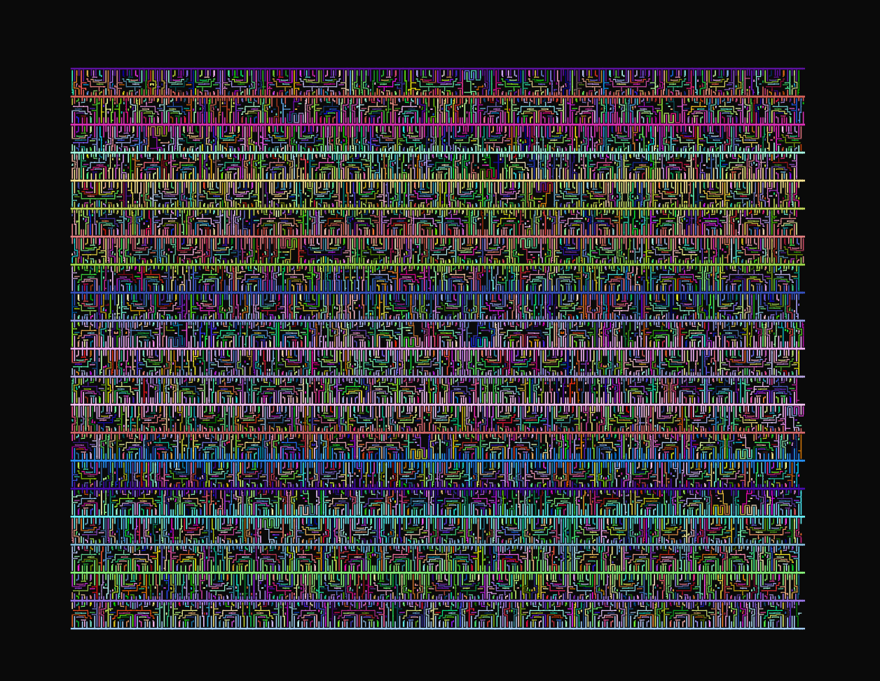 |
| layer 49 – metal 1 |
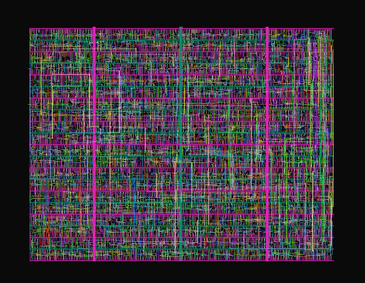
 |
| layer 31 – metal 4 |
Looks promising.
Step 2 – combine segments together into nets that can span multiple layers
- For every segment of every layer I wrapped it into a new Net. These nets, apart from containing rectangles, also have:
- a name (autogenerated or using a predefined name if it starts at a know point, eg. one of the I/O pins)
- a set of vias they go through (initially empty)
- For every via in the design:
- I found all rectangles that connect to it (on the neighbouring metal layers) and the nets in which they’re contained. I then appended that via to the nets’ via set.
- I then join all nets by their common vias:
- For every net in the design:
- For every via in this net:
- I merge the net with all other nets that contain this via.
Step 3 – map nets to cells
- For every cell of the design, I calculated the absolute coordinates of the I/O pins that I mapped out earlier.
- For every I/O pin, I find a net that contains it on a rectangle in metal layer 1. I map this net as that pin for this cell. I also back-map this the other way around – what pins on what cells is a given net connected to.
Netlist Analysis

- All the D-flip-flops are clocked from the outside clock line synchronously
- All the D-flip-flops are daisy-chained together via AND gates.
- All the only other use of the D-flip-flops data outputs, apart from daisychaining, is to drive a large combinatorial network of logic gates that outputs the ‘unlocked’ signal.